86-755-2780 6973
Info@niksoupcb.com


|
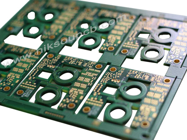
Technical Capacity | |||
|
Layer Counts |
1-24L |
Min Board Thickness(2-layer) |
0.2mm |
|
Max board size(mm) |
1200x400mm |
Min Board Thickness(4-layer) |
0.4mm |
|
Max copper |
12oz |
Min Inner-layer Thickness |
0.1mm |
|
Min Trace |
0.075mm |
Min Pad Ring |
0.1mm |
|
Min Clearance |
0.075mm |
Min Hole Location Tolerance |
±0.075mm |
|
Min Hole Size(laser hole) |
0.1mm |
Min Hole Size Tolerance |
±0.05mm |
|
Board Twist |
≤ 1° |
Min Outer Dimension Tolerance |
±0.1mm |
|
Base Material |
FR4,High-TG FR4,CEM3,aluminum,High Frequency(Rogers,Taconic,Aron,PTFE,F4B) | ||
|
Surface Finish |
HAL,lead-free HAL,ENIG,Plated Gold,Immersion Gold,OSP | ||
|
Soldermask |
Green, Blue, Black, White, Yellow, Red, Matt Green, Matt Black, Matt Blue | ||
|
Silkscreen |
White, Black, Blue,Yellow | ||
|
Acceptable File Format |
Gerber file,Powerpcb,CAD,AUTOCAD,ORCAD,P-CAD,CAM-350,CAM2000 | ||
|
Certificate |
ROSH,ISO9001,UL | ||
|
Standard |
2-layer samples in about 3 days | ||